November 11, 2020
The pins on the blue pill are something else entirely. There is no handy sequential "D" numbering on the silkscreen and the board is not laid out in the same way as the maple-mini.
What you are probably itching for now are some diagrams and tables, so here we go.
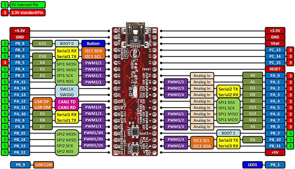
Here is the maple-mini pinout. Note that somebody got the idea of giving software names to the pins as shown whith white text on a blue background (such as "PC_13"). This would have the advantage of the same name for a given GPIO pin regardless of what connector pin it was routed to on the board. Both this and the name "D14" for the same pin would have their own advantages.
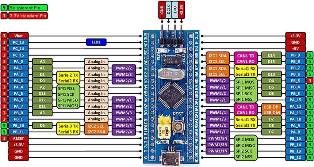
Here is the blue pill pinout. Note that we now have a handy SWD connector on the end. Also note that there is virtually no correspondence to signal locations on the maple-mini and no handy sequential "D" numbering on the silkscreen.
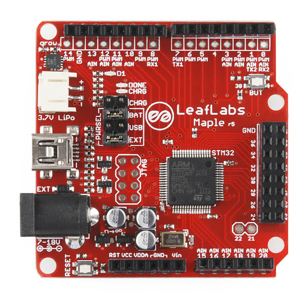
The Maple board is an entirely different beast. Perhaps because it is much rarer in the wild, I haven't found an equivalent handy diagram like the above. You have to go with the silkscreen "D" number markings and the following tables (from the original Leaf Labs documents).
Here is the "master pin map" for the Maple mini:
| Pin | GPIO | ADC | Timer | I2C | UART | SPI | 5 V? |
|---|---|---|---|---|---|---|---|
| D0 | PB11 | 2_SDA | 3_RX | Yes | |||
| D1 | PB10 | 2_SCL | 3_TX | Yes | |||
| D2 | PB2 | Yes | |||||
| D3 | PB0 | CH8 | 3_CH3 | ||||
| D4 | PA7 | CH7 | 3_CH2 | 1_MOSI | |||
| D5 | PA6 | CH6 | 3_CH1 | 1_MISO | |||
| D6 | PA5 | CH5 | 1_SCK | ||||
| D7 | PA4 | CH4 | 2_CK | 1_NSS | |||
| D8 | PA3 | CH3 | 2_CH4 | 2_RX | |||
| D9 | PA2 | CH2 | 2_CH3 | 2_TX | |||
| D10 | PA1 | CH1 | 2_CH2 | 2_RTS | |||
| D11 | PA0 | CH0 | 2_CH1_ETR | 2_CTS | |||
| D12 | PC15 | ||||||
| D13 | PC14 | ||||||
| D14 | PC13 | ||||||
| D15 | PB7 | 4_CH2 | 1_SDA | Yes | |||
| D16 | PB6 | 4_CH1 | 2_SCL | Yes | |||
| D17 | PB5 | 1_SMBA | |||||
| D18 | PB4 | Yes | |||||
| D19 | PB3 | Yes | |||||
| D20 | PA15 | Yes | |||||
| D21 | PA14 | Yes | |||||
| D22 | PA13 | Yes | |||||
| D23 | PA12 | 1_ETR | 1_RTS | Yes | |||
| D24 | PA11 | 1_CH4 | 1_CTS | Yes | |||
| D25 | PA10 | 1_CH3 | 1_RX | Yes | |||
| D26 | PA9 | 1_CH2 | 1_TX | Yes | |||
| D27 | PA8 | 1_CH1 | 1_CK | Yes | |||
| D28 | PB15 | 2_MOSI | Yes | ||||
| D29 | PB14 | 3_RTS | 2_MISO | Yes | |||
| D30 | PB13 | 3_CTS | 2_SCK | Yes | |||
| D31 | PB12 | 1_BKIN | 2_SMBA | 3_CK | 2_NSS | Yes | |
| D32 | PB8 | 4_CH3 | Yes | ||||
| D33 | PB1 | CH9 | 3_CH4 |
And here is the "master pin map" for the Maple:
| Pin | GPIO | ADC | Timer | I2C | UART | SPI | 5 V? |
|---|---|---|---|---|---|---|---|
| D0 | PA3 | CH3 | 2_CH4 | 2_RX | |||
| D1 | PA2 | CH2 | 2_CH3 | 2_TX | |||
| D2 | PA0 | CH0 | 2_CH1_ETR | 2_CTS | |||
| D3 | PA1 | CH1 | 2_CH2 | 2_RTS | |||
| D4 | PB5 | 1_SMBA | |||||
| D5 | PB6 | 4_CH1 | 1_SCL | Yes | |||
| D6 | PA8 | 1_CH1 | 1_CK | Yes | |||
| D7 | PA9 | 1_CH2 | 1_TX | Yes | |||
| D8 | PA10 | 1_CH3 | 1_RX | Yes | |||
| D9 | PB7 | 4_CH2 | 1_SDA | Yes | |||
| D10 | PA4 | CH4 | 2_CK | 1_NSS | |||
| D11 | PA7 | CH7 | 3_CH2 | 1_MOSI | |||
| D12 | PA6 | CH6 | 3_CH1 | 1_MISO | |||
| D13 | PA5 | CH5 | 1_SCK | ||||
| D14 | PB8 | 4_CH3 | Yes | ||||
| D15 | PC0 | CH10 | |||||
| D16 | PC1 | CH11 | |||||
| D17 | PC2 | CH12 | |||||
| D18 | PC3 | CH13 | |||||
| D19 | PC4 | CH14 | |||||
| D20 | PC5 | CH15 | |||||
| D21 | PC13 | ||||||
| D22 | PC14 | ||||||
| D23 | PC15 | ||||||
| D24 | PB9 | 4_CH4 | Yes | ||||
| D25 | PD2 | 3_ETR | Yes | ||||
| D26 | PC10 | Yes | |||||
| D27 | PB0 | CH8 | 3_CH3 | ||||
| D28 | PB1 | CH9 | 3_CH4 | ||||
| D29 | PB10 | 2_SCL | 3_TX | Yes | |||
| D30 | PB11 | 2_SDA | 3_RX | Yes | |||
| D31 | PB12 | 2_SMBA | 3_CK | 2_NSS | Yes | ||
| D32 | PB13 | 3_CTS | 2_SCK | Yes | |||
| D33 | PB14 | 3_RTS | 2_MISO | Yes | |||
| D34 | PB15 | 2_MOSI | Yes | ||||
| D35 | PC6 | Yes | |||||
| D36 | PC7 | Yes | |||||
| D37 | PC8 | Yes | |||||
| D38 | PC9 | Yes | |||||
| D39 | PA13 | Yes | |||||
| D40 | PA14 | Yes | |||||
| D41 | PA15 | Yes | |||||
| D42 | PB3 | Yes |
Tom's Computer Info / tom@mmto.org