March 10, 2025

STM32F429 Discovery Kit - Clocks

If you want to know about clocks, check section 6.2 of the TRM.

Serial and USB clocks

We first began with our F429 board by just running the F411 build of Hydra. This worked, but the serial port was not running at 115200. Some trial and error led to the discovery that it was running at 38400 baud. Notice that this is off by a factor of 3 exactly. We did some hackery to get the serial port to work at 115200 (by telling it that the bus clock was running at 16 Mhz rather than 48).

But the USB system needs a clock at 48 Mhz and there are no two ways about it. We have to "make it so". And the USB system on our F429 board does not work, so this clearly needs to be addressed.

The clock diagram

The following, from page 152 of the TRM tells you most of what you need to know. The rest of the details are in chapter 5 of the TRM

Important details

The 429 discovery board has an 8 Mhz crystal. This is the start of our problems. The F411 "black pill" has a crystal that is marked on my board as 25 Mhz, and this is what the schematic shows as well. So why do we get a 38400 baud rate? Well, the truth is that we actually get a rate of 115200 * 8/25 = 36864, but that is somehow "close enough" to work with picocom at 38400. We are only off by 4 percent.

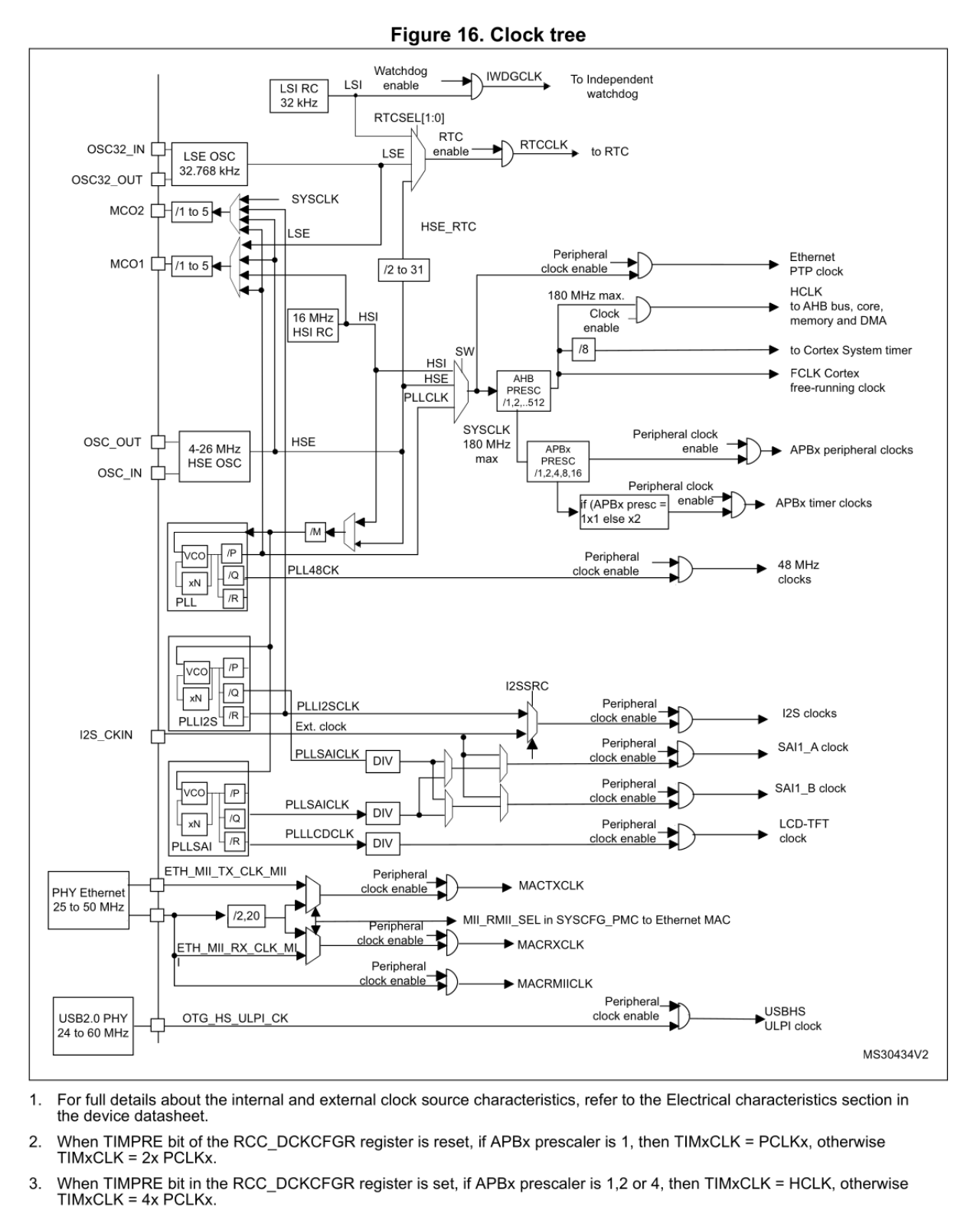
The F411 has a max CPU clock of 100 Mhz (but we run it at 96 Mhz). The F429 has a max CPU clock of 180 Mhz. We won't be able to run it that fast and get USB to work, because of the need for that 48 Mhz clock. It looks to me that 168 Mhz will work out. The actual truth is that an intermediate clock running at twice that rate (336 Mhz) can be divided by 7 to give us 48, and when divided by 2 gives us 168.

As a matter of interest 336 factors to 2 * 2 * 2 * 2 * 3 * 7.
We can divide it neatly to get 16, but not 32.
We might like to try 192 Mhz as a CPU clock, and we might get away with it, but it would be over the legal limit of 180.

What about MCO1 and MCO2

See section 6.2.10 of the manual. We have the ability to output a selected clock on a chip pin. We have two pins (MCO1 and MCO2) which are available on some GPIO as an alternate function. It takes a lot of digging, but apparently these are on:
MCO1 - PA8 as AF 0
MCO2 - PC9 as AF 0

All GPIO come up with AF 0 selected, so we may not need to do anything to get MCO output on these pins.

These are side by side on the P1 connector on the discovery board.

Amazingly, these are configured by the RCC "conf" register at offset 8. Each has a 3 bit field to configure a prescaler (1 to 5 as per the block diagram above). Each also has 2 bit field to select one of four sources.

The idea is to set up these MCO output and use a scope to look at the clocks that are generated!


Feedback? Questions? Drop me a line!

Tom's Computer Info / tom@mmto.org