A quick rundown of what the STM32F103 offers:
ARM Cortex M3 running at 72 Mhz (32 bit).
64K of flash.
20K of ram.
USB interface
30 gpio pins
9 analog pins (12 bit, 1 us).
3 uarts
4 timers (each with 4 channels, so 16 timer driven pins)
other peripherals (CAN, I2C, SPI, Watchdogs ...)
Similar boards using the STM32F103CB are the Naze32 and Flip32+ boards. What I have is sometimes called a "blue pill". There is also a "red pill". Rumor has it you can power it with anything from 2.0 to 3.3 volts
Compare this to an Arduino Uno with 32K of flash, 2K of ram, and an 8 bit AVR risc running at 16 Mhz (for $25). 6 analog inputs (10 bit) and 14 gpio pins. I hear you already, but what about the Arduino IDE -- well a plugin for this little ARM board is apparently available for the Arduino GUI, not that I care all that much.
It is even more interesting to compare this to the 8751 processors that I used to be fond of. We used them with 32K external eprom, and if we felt generous, wired up an 8K static ram as well. These ran at 11 Mhz, but were not RISC, so the equivalent clock rate was perhaps 2 Mhz. We could not use gcc, we used offbeat commercial C compilers.
While you are comparing, consider the STM32 Discovery boards from ST electronics. You can get these from Digikey or Newark for about $10. If you are going to be spending this much money, look for a chip with 128K of flash. There are a whole family of STM32 variants.
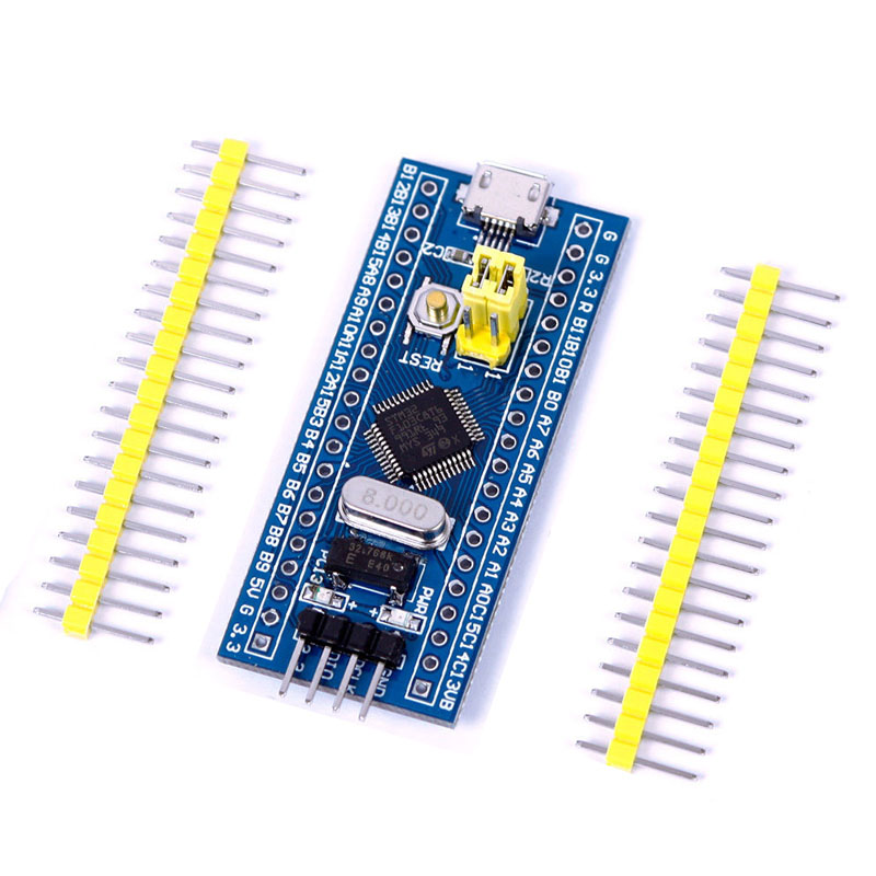
the STM32F103C8T6 chip
40 pins (20 on each side) on 0.1 inch centers.
a 4 pin header
Two yellow jumpers
An 8 Mhz crystal
A 32768 Hz oscillator
a 3.3 volt regulator (probably U1 on back of the board)
a power LED
an LED labelled "PC13"
a reset button.
The yellow jumpers are connected to the processor BOOT0 and BOOT1 lines and can be set to connect these either to ground (in the 0 position) or to a pullup to 3.3 volts (in the 1 position). The jumper away from the reset switch is BOOT0. There are 3 possible configurations:
BOOT0 = 0, BOOT1 = any - boot program from flash memory (normal operation)
BOOT0 = 1, BOOT1 = 0 - boot from system memory (run bootloader)
BOOT0 = 1, BOOT1 = 1 - boot from SRAM (how do we get a program there?)
The four pin header on the end is something called an SWD port. This is sort of a poor-man's JTAG. It can run at 40 Mhz and be used for downloading software into flash (like new bootloaders) as well as debugging. More on this elsewhere.
Tom's Computer Info / tom@mmto.org