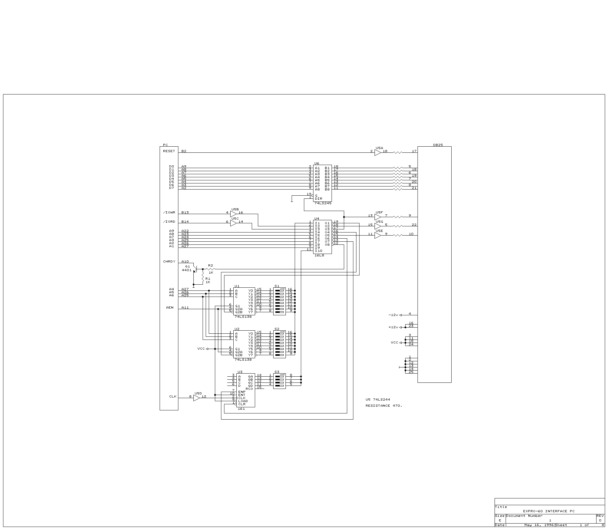
Here is a JEDEC file for the GAL device on the board (actually the schematic shows a PAL16L8, but typically a GAL16V8 is used). You could use this to burn a PAL and along with the schematic you could build a board -- but if I was going to do that, I would look at the hand drawn schematic that does not use a PAL, but instead uses a couple of readily available TTL chips. No GAL device buying or burning would be required.
It turns out that the GAL (PAL) is a fairly simple thing. It is entirely combinatorial (simple AND and OR logic) with no states or registers. After a bit of educating myself about Jedec files and the format pertaining to the GAL16V8, I came up with these equations:u1io = a9 + a8* + a7* cable(22)-write = iowr** + addr** + a3* + a2* + a1 cable(9)-read = addr** + iord** + a3* + a2* + a1 u2io = a9 + a8* + a7 cable(10)-2E0 = addr* | iowr* | a3 | a2 | a1 clr-161 = addr* | a3 | a2 | a1* | ( iowr* + iord* ) enp-161 = addr* | wait | a3 | a2 | a1* | ( iowr* + iord* ) iordy = addr* | wait | a3 | a2 | a1* | ( iowr* + iord* )Of course to make any sense of this, you need to know what names I assigned to various pins on the PAL, and so here you go:
pin 1 - addr*
pin 2 - iowr*
pin 3 - iord*
pin 4 - a9
pin 5 - a8
pin 6 - a7
pin 7 - a3
pin 8 - a2
pin 9 - a1
pin 11 - wait
pin 12 - iordy
pin 13 - enp-161
pin 14 - clr-161
pin 15 - cable(10)-2E0
pin 16 - u2io
pin 17 - cable(9)-write
pin 18 - cable(22)-read
pin 19 - u1io
First, address decoding. This is a cooperation between the GAL and the pair of LS138 decoders. First let us say some things about the ISA bus. The ISA bus only works with 10 bits of address information for IO transactions, so you have ports from 0 to 0x3ff and need only look at A0 to A9. The decoding on this card works like this. The GAL looks at the upper 3 bits, namely A9, A8, and A7. If it sees 100 it asserts u1io. If it sees 101 it asserts u2io. This enables either u1 or u2 to decode the next 3 address bits (A6, A5, and A4). For the usual address of 0x2e0, the bits are 10_1110_0000. So the upper bits are 101 and the U2 decoder is enabled. The next 3 bits are 110 which will cause pin 9 (Y6) to go low. The switch S2 (or a jumper) should be set to select this signal and it goes back to the GAL on pin 1 as "ADDR*"
Second, wait states. This is what the LS161 chip and the signals enp-161, clr-161, wait, and iordy are all about. I don't care about these, and am not going to go into detail. All the information you need to sort this out is there for you on the schematic and the PAL logic. The idea of course is to manipulate the IORDY signal on the ISA bus such that the card will work on fast buses.
Third, and by far the most interesting are the three signals to the cable.
First note that pin18 -- cable(9) write also controls the DIR signal for the LS245 bus transceiver. When this signal is low, data is moving from B to A (from the EMUP to the ISA bus), so a read is going on. Otherwise we are writing. As it turns on, we support writes to 0x2e0 and 0x2e2, but we only support reads from 0x2e2. Look at these equations for the read/write signals. We already have "ADDR" telling us that A9 to A4 match our jumpered address (0x2e0). These equations match the low address bits A3, A2, and A1 and are looking for 001, so 0x2e2 overall. What about A0 you might ask -- this is something for the reader to investigate in the ISA bus documents.
cable(22)-write = iowr** + addr** + a3* + a2* + a1
cable(9)-read = addr** + iord** + a3* + a2* + a1
So, pin 9 on the cable is asserted if we have a write to 0x2e2. Pin 22 on the cable is asserted if we have a read from 0x2e2.
What about the other signal on the cable (pin 10). This is asserted (active low) if we have a write to 0x2e0. Nothing happens if we read from 0x2e0, this is a write only address. The equation is as follows:
cable(10)-2E0 = addr* | iowr* | a3 | a2 | a1Notice that this is all "OR" logic. If we invert all the signals and change the operators to "AND" we get:
cable(10)-2E0 = addr** + iowr** + a3* + a2* + a1*Compare this to the cable(22)-write equation. No telling why it was not just written and implemented this way in the GAL.
Tom's Electronics pages / tom@mmto.org