A brief note on the "WR*" annotation. This is one of several common ways to indicate an "active low" signal. Another way would be "WR\" and another is to place a bar over "WR" (impossible using ascii characters).
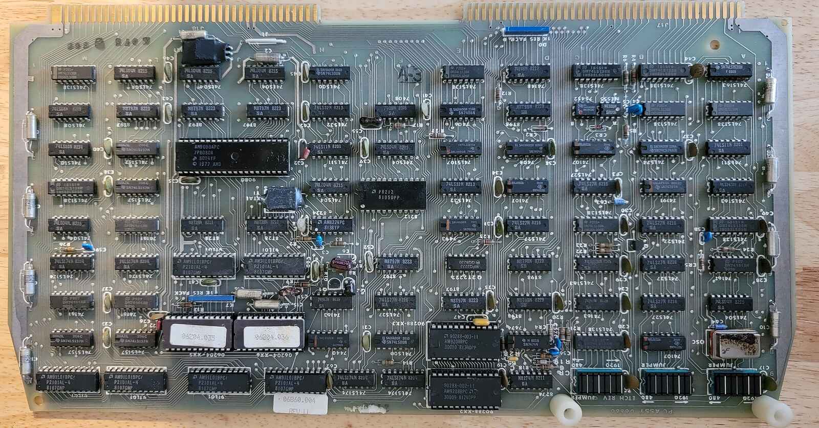
The 8 data lines are buffered by a pair of 8T28 chips. The Entrex engineers do something curious here, they generate a pair of 8 bit data bus signals that I call DI and DO (for data in and data out). You will note that if you look at the processor ROM chips (UJ8 and UK8) they are connected to the DI bus -- which makes sense as they will provide data going in to the processor.
The LS138 had 6 inputs. The most important are the 3 address inputs. These are connected to A10, A11, and A12 on the address bus. The other three are what I call "game on" signals, two are active low inputs and the others are active high. These must be satisfied for this chip to do anything at all. We will discuss these later.
Consider the 3 address lines A10-A12. In a 16 bit word these are located as follows:
000x xx00 0000 0000
If xxx are 000 we decode address 0 (hence the first ROM).
if xxx are 001 we decode address 0400 (the second ROM).
Continuing in this was, we can work out the address map as seen by the 8080
0x0000 - ROM0
0x0400 - ROM1
0x0800 - sel_08
0x0C00 - sel_0C
0x1000 - sel_10
0x1400 - sel_14
0x1800 - sel_18
0x1C00 - sel_1c
The low bits (A0 to A9) select from one of 2^10 addresses (1024), which makes perfect sense as we have 2708 ROM chips which are 1K by 8. As for the other six selects, we will learn more later (we hope).
What about the three high bits I hope you are asking. Unless these are qualified in some way by the "game on" signals, these are "don't care". That means that this address map is repeated 8 times in the 16 bit address space. This is common practive and entirely harmless. However, this is not what is done here. The game on signals involved A13, 14, and A15 and require them to be zero. In addition, the DBIN* signal from the processor makes this decoder only active for processor reads (which is somewhat unusual).
The game here is to grab processor status signals from the data bus. The 8 bit input to the 8212 is the DO bus (data coming out of the processor). Pin 11 tells this chip to latch the contents of the data bus at the proper time when the processor status signals are present Intel provided a dedicated companion chip for the 8080 to latch this information and massage it into a set of vital signals. This was the 8228 chip. The Entrex engineers chose not to use this part, although they did use the 8224 clock generator chip. In the Intel 1975 8080 Microcomputer systems Users Manual, in chapter 3, they talk about all of this and in Figure 3.5 they present a schematic for generating these vital signals using more common parts.
The decoder for this/these is the LS138 chip at UM1. This decoder has some other LS138 buddies as UB1 and UC1. We know about the game with these decoders from the discussion above, so let's look at what is specific about this one.
The 3 address lines are A9, A10, and A11. This leaves A0 to A8 to select individual bytes from the ram array itself, but the careful reader will notice that this allows 512 bytes and our chips only have 256. There is something sneaky however going on with A8 -- it is routed to pin 17 on both RAM chips. Pin 17 is an active high chip enable, so the chips will only respond if A8 is high. Good so far.
The Address lines A9, A10, A11 must all be high to trigger the pin 7 (RAMSEL*) output from the UM1 decoder. So we are all ones so far, what about A12 ... A15. These are all used as follows with the three "game on" signals for the LS138.
A12 and A13 drive the E3 input, so both must be high
A14* drives the E1* input, so it must be high
A15** drives the E2* input, so it also must be high
All told, this makes the processor RAM respond at address base 0xff00, and looking at the disassembled code from the ROMs, this is consistent. The ROMs place the stack base at 0xFFD0, and place variables at 0xFF00 to 0xFF22 as well as 0xFFF8 to 0xFFFD, all within the decoded range we just worked out.
Notice though that this decoder says nothing about processor states. Something else must ensure that RAM does not respond when IO reads take place for example. My bet is this -- when IO reads and writes take place, the upper 8 bits of the address bus is zero and this decoder will not respond.
The UB1 decoder gets DBIN and INP* to its active low "game on" inputs.
The UC1 decoder gets WR* and OUT* to its active low "game on" inputs.
So UB1 handles "IN" instructions and UC1 handles "OUT" instructions.
Ignoring the low 3 bits would suggest that the IO ports are spaced 8 bytes apart in the address space. Ignoring two high bits (A6 and A7) would suggest that we have 4 identical copies of the IO ports at 0x00, 0x40, 0x80, and 0xc0. For whatever reason the ROM code uses the set at 0x40, and we see accesses to these ports:
; IN instruction addresses:
;       40
;       48
;       50
;       58 - unused
;       60 - unused
;       68
;       70
;       78
; OUT instruction addresses:
;       40
;       48 - unused
;       50
;       58
;       60
;       68
;       70 - unused
;       78
;
; OUT port 40 -- written in just one place
; OUT port 50 -- only 1, 2, 4 written
; OUT port 58 -- tricky, but most bits used
; OUT port 60 -- tricky, but most bits used
; OUT port 68 -- only ever is 0xff written
; OUT port 78 -- all 8 bits are used
Now I have relabeled the signals for the port select lines and here is what I see (I have carefully searched the schematic looking for things each select might control, but it is certainly possible I have missed things).
outp_78 -- goes to interface board
outp_70 -- goes to interface board, but unused in ROM
outp_68 -- goes to interface board
outp_60 -- goes to interface board
outp_58 -- goes to interface board
outp_50 -- goes to magic 555 section (no data) also to N/C in backplane
outp_48 -- goes offboard to FDC (unused in ROM)
outp_40 -- goes to nonsense section (no data) also offboard to FDC


inp_78 -- goes to interface board
inp_70 -- goes to interface board
inp_68 -- goes to interface board
inp_60 -- goes to FDC (unused in ROM)
inp_58 -- goes to FDC (unused in ROM)
inp_50 -- goes to keyboard section (data)
inp_48 -- goes to keyboard section (status)
inp_40 -- goes to RAM expansion board
It seems odd that an input port would be coming from a RAM expansion board, but anything is possible I suppose. Maybe just reading the port does a reset. Such things have been done.
The ram has two sides. On one side the processor can write into it. The processor cannot read the video ram. On the other side the video circuit reads from it. Interesting complexity arises from the need for some kind of arbiter circuit. If the CPU could simply write at any old time, it would conflict with the video circuit and yield glitches and trashy display and who knows what.
Some notes in my ROM disassembly state:
; Display memory seems to be at 0xc000, but there is something
; at 0xf000 that gets cleared at start up.
The heart of it is two chips, a pair of 8T98 chips and one section of an LS74.
First the LS74. A pulse on pin 3 (UD8_3) would clock a "1" into this flip flop. A read of port 0x50 would clear it. It provides a bit that can be read on port 0x48 (see below). I would almost suspect this to have other connections (or else it is useless). It is the kind of thing that might be set up to generate an interrupt (and then the read would clear the interrupt). These connections need careful double checking.
The read on port 0x48 gives what looks like 4 bits of status.
The bits are: 0F00 0abc -- where:
F is the bit from the LS74 flip flop that was just discussed.
a is from J17_46
b is from J17_44
c is from J17_42
The read on port 0x50 gives 8 bits of data:
d7 - J17_48
d6 - J17_50
d5 - J17_52
d4 - J17_54
d3 - J17_56
d2 - J17_58
d1 - J17_60
d0 - J17_62
I believe pin 15 is connected to pin 1 on UD6, though the schematic does not show this.
And now a curious side note. I took a look at the keyboard signals on the backplane. One signal routes to J17_76 and seems to be special in some way. I thought it might be routed to the interrupt controller, but I was wrong. I goes to the keyboard and is driven by the mystery 555 section of the schematic. Who would have guessed? And who knows just what the mystery 555 section is up to?
In addition a read from port 0x50 delivers a pulse to this 555 section (to the TR pin on the 555 ultimately). Reading port 0x50 also fetches 8 bits of data from the main keyboard section. It almost looks as if the 555 is some kind of watchdog timer, but that is a wild speculation and I am too lazy right now to study this circuit in detail.
The lower part of the "mystery" section shows the circuit. Eight possible interrupt sources go to an LS148 chip which is designed to announce the interrupt and indicate which source is the highest priority interrupter. I am betting that one of these is the keyboard. Why? Because the ROM shows an interrupt handler (RST-4) to handle keyboard interrupts.
The other part of the interrupt circuitry in the "mystery" section is the 8T98 at UD2. This responds to the sINTA signal from the processor status signal and places the proper RST instruction on the data bus to vector the interrupt (if such can be called on an 8080).
Note that the ROM shows several interrupt handler routines. There are 4 as near as I can tell, for RST-3, RST-4, RST-5, and RST-6. The one for RST-4 handles keyboard interrupts.
Here is a "round 2" on the interrupt circuit. The first player is the LS148 chip. This chip is essentially custom made for use in processor interrupt generation circuits. The basic idea is that the chip has 8 inputs (for 8 possible different interrupt sources). When any one of them gets pulled low, somebody somewhere wants to interrupt the processor. The processor has a single, active high, interrupt request line. The LS148 has an output on pin 14 (GS) that goes low when one or more of those 8 interrupt request lines gets pulled low. This signal gets inverted so it is active high and that is the interrupt signal to the processor.
But there is more. What if more than one request line is pulled low to request an interrupt. The interrupt signal to the processor will indeed get yanked. The LS148 is called a "priority encoder" because it has 3 bits of output that indicate what line got yanked. If more than one line got yanked, those 3 bits indicate the highest priority line where pin 4 (input 7) is the highest and pin 10 (input 0) is the lowest. Sort of the inverse of what an LS138 does.
There is even more. The processor so far has only gotten the single "INT" line yanked high, but it has no idea which of the 8 sources is interrupting. What the 8080 does is to run an INTA (interrupt acknowledge) cycle next. The goal of this is to fetch a single byte instruction and execute it. The 8080 has provided the RST instruction for just this purpose.
The bit pattern for the RST instruction is "11xxx111", i.e. all ones except for the 3 bits indicated by "xxx". You may guess where this is going. If we can arrange to insert the 3 bits from the LS148 here, we can tell the processor which interrupt source requested the interrupt. The processor then effectively does a "CALL" instruction to address "xxx" * 8. So the first 64 bytes of memory for an 8080 ROM will have the interrupt handlers for sources 0-7. Slick, eh?
Back at the schematic we see UD2 (an 8T98 -- an inverting buffer). Its sole purpose it to place the "xxx" onto the data bus during an INTA cycle. Interestingly it only drives lines D3, D4, and D5. Something else must pull the remaining lines on the data bus high to provide the ones. Maybe they float high (never a good design) or maybe they have pullups that I am too lazy to search for on the schematic.
A quick side note from the ROM code. We have reason to believe that the RST-4 handler is responding to keyboard interrupts. Call this a theory.
Now, what about those 8 interrupt sources? First consider that the 8T98 inverts the signals from the LS148. This is because the LS148 indicates source 7 by "000", so inverting these bits makes it "7" again. This could all have been handled without the inversion by rerranging the tables in the ROM, but they need a driver chip here anyway, so why not use one that inverts and avoid the confusion.
Now, what about the keyboard interrupt? We can track down the line that produces RST-4 simply as pin 1 on the LS148. But we now see a very strange thing. We see this line with a pullup resistor to Vcc and no other connection. This means one of two things. Either they never want an interrupt to be generated (unlikely if we really desire keyboard interrupts) or there is an errata on the schematic. My theory is the latter. I think this signal, as well as being pulled up, is also driven by pin 6 on UD8.
UD8 is a flip flop. A pulse on pin 3 (I believe there is an errata there also as it is shown as unconnected) will clock a "1" into the flip flop. This will make the Q* output go low (yielding a "1" bit in the status register read in port 48 because it is driven by an inverting 8T98 again). The Q* input (pin 6) would be just the thing to pull the LS148 line low to produce the interrupt we expect. When the cpu reads from port 50, this resets the flip-flop and clears the interrupt.
The other inputs to the LS148 go to the card edge as follows:
IRQ0 (pin 10) - to FDC board 53
IRQ1 (pin 11) - to FDC board 55
IRQ2 (pin 12) - to FDC board 57
IRQ3 (pin 13) - not connected
IRQ4 (pin 1) - keyboard (see above)
IRQ5 (pin 2) - to interface board 66
IRQ6 (pin 3) - to interface board 64
IRQ7 (pin 4) - to interface board 67
The IRQ4 input is not routed off board. We don't care about the 3 floppy interrupts. But the three interface board interrupts are of interest.
Note that RST-0 is a cold start reset. Would the floppy board ever want to cause one of those? It seems unlikely, but one never knows. A switch to ground on this pin would yield a reset, so maybe the floppy had a reset button. The ROM has no code for RST-1 or RST-2 from the FDC.
The rom does have code for IRQ5 and IRQ6 from the interrupt board. If IRQ7 ever happens, it branches to a hard reset.
I located and renamed the 3 signals as follows:
IRQ5	P15_66 - interface
IRQ6	P15_64 - interface
IRQ7	P15_67 - printer (but weird)
The first two are indeed from the host interface logic and will need attention. The last (IRQ7) is from the printer section and seems silly. As it is currently set up it is driven by a bit that is set by a write to port 0x60. I don't see how that would be useful in any way, so perhaps this is an errata. Given that code in the ROM ignores it and that we don't have a printer board (or a printer), it isall pretty moot.
As you might guess, the game here is routing address signals to the video ram chips. The "A" signals are addresses from the CPU, the "B" signals are from the video display subsystem counters. The signal that selects which is which is on pin 1. It is low to get A, high to get B. I will call it VCPUSEL* since it selects CPU access to video ram when low.
This signal originates from the LS74 dual flip flop at UB3 (pin 5). Closely related is the signal VWR*, which is the active low "and" of WR* and VCPUSEL* and indicates (to the video ram) that the CPU is performing a write.
On the Entrex board, they decide what drives the address lines on the video ram.
Now, some funny shenanigans go on with the upper address bits before they get fed to the selector. The cpu address bits that it. A12 and A13 get inverted. Bearing this in mind, lets look at UM4, which is an LS138 that generates the chip selects for the video ram array. A8, A9, and A10 provide the 3 address "selector" bits, so there is no funny business there. Now lets look at the three "game on" inputs. A14 and A15 go to a NAND that drives the active low E2 input (this will require A14 and A15 to both be "1"). OK so far.
A11 and A12* and A13* all go to an "and" (a 3 input "and" built from a pair of two input "and" gates). The output of this and drives the active high E1 input on the LS138. The end result of this is to require A11 = 1, A12 = 0, and A13 = 0. This means the processor will "see" the video ram starting at 1100_1000_0000_0000 or 0xc800. Or so you might thing, however there is more monkey business The actual value of A11 is not what gets to the 3 input "and", the LS157 selector input for the CPU is hard wired to Vcc (a "1" value).
The end result of this is that the CPU sees two copies of video ram. One is at 0xc000 and the other is at 0xc800. This is exciting because we see the ROM code writing to display ram at address 0xc0000.
As a final note -- the board can be jumpered in either 1920 or 480 character mode. You can satisfy yourself that this has no effect whatsoever on what was just worked out in the prior paragraphs. But as long as we are talking about this, here is how that all works out. The standard product supports 480 characters (12 lines of 40 characters). 480 characters fit nicely into the 512 bytes of video ram provided by four 9101 chips and all is good.
The optional 1920 mode (24 lines of 80 characters) requires 4 times as much video ram (16 9101 chips in all, 4 on the main processor board, and 12 on the optional "RAM" expansion board). This would give 2048 bytes of video ram and that would nicely take care of the 1920 bytes required. I don't intend to say much more than this about the 1920 mode. There are a bunch of jumpers on the processor board that need to get swapped around to configure for this (along with the installation of the ram expansion board).
I don't actually intend to dig too deeply into the circuitry that continually scans the video ram and generates video using the character roms. Once I understand how the CPU accesses the video ram, I'll be satisfied. Not that all that wouldn't be interesting (and perhaps even exciting), but we have other pressing matters, Such as the interface card. The arbiter that decides when and if the CPU is allowed to write to video ram would be interesting to understand.
A peek at the backplane schematic though shows an 8 pin connector devoted to the "terminal" (i.e. monitor).
The rom writes in a loop to some block that starts at 0xf000. What the heck is this and what hardware supports it? Could this be on the interface card?
What clock runs the video timing? We have a 555, but it doesn't look to me like it is even running as an astable (i.e. an oscillator). We have the processor crystal at 18.0 Mhz. Does that get tapped for the video timing? It must. I don't what else could be going on.
Tom's Computer Info / tom@mmto.org