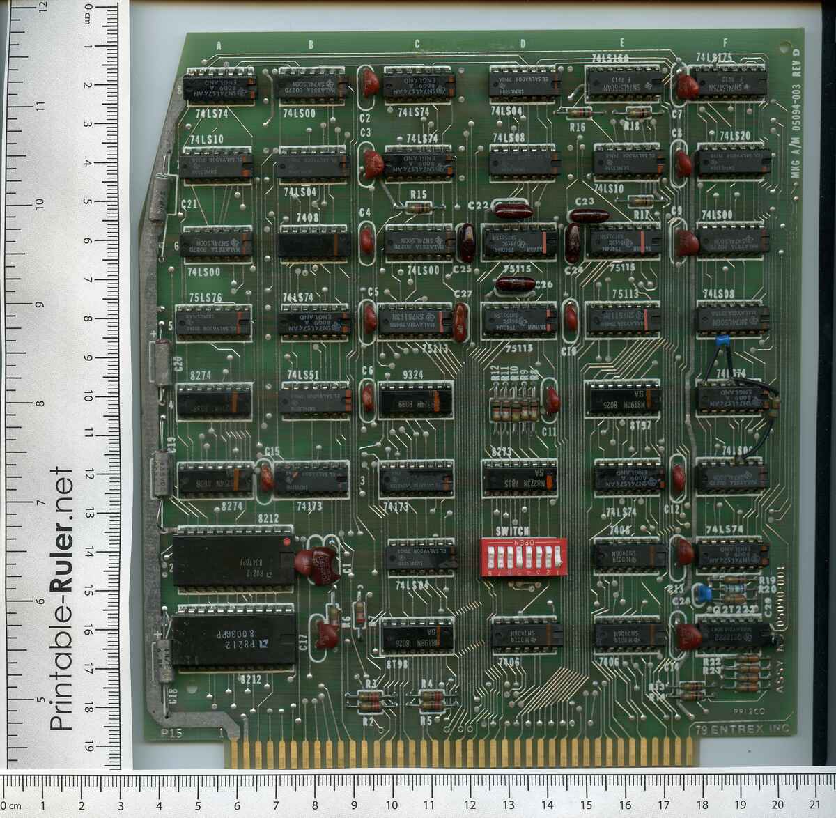
This is my "discussion" of the circuit for the above board. I am trying to put into words what I am able to learn by studying the schematic and assigning helpful names to signals.
AJ did a nice job on the schematic with signals flowing from left to right. The right side ends in two 8212 device (8 bit latches) driving 16 open collector outputs (7406 devices). These all drive signals on the P15 edge connector that AJ has designated "printer".
So we may be able to call this a dual function IO board. It drives the printer (and we will sort of ignore that) and it provides data from the pair of interface connectors (maybe).
The 8273 is a 10 bit serial in, parallel out shift register.
The 8274 is a 10 bit parallel in, serial out shift register.
We get a pair of 8274 on the board, but only one 8273. This seems a bit surprising, but will no doubt make sense once we unravel the design (or else I just missed a second 8273).
These chips promise to be the heart of the matter given that the outside world interface for the Entrex is some kind of unique serial protocol.
Once we label the data bus signals, we discover that both 8274 are connected (albeit with some strange issues) to the DO bus on the parallel side, which sort of makes sense. What isn't clear is what causes the 8274 to latch (capture) data from the DO bus. Each chip has 2 control signals S0 and S1 with the following 4 states:
S0 = low, S1 = low -- hold
S0 = low, S1 = high -- clear
S0 = high, S1 = low -- load
S0 = high, S1 = high -- shift
S0 is pulled high (to Vcc) on both, so we just get the last 2 cases, load or shift. So, what causes S1 to go low and data to be loaded? Both chips are controlled by the same signal u8_11, which I am going to rename LOAD* as an active low signal.
IN 0x78 -- enables data read from UE4 (8T97)
	    This looks like status information (5 bits, 3 high, 2 low)
IN 0x68 -- enables data read from UB3 and UC3 (both 74173)
	    This looks like actual data

OUT 0x78 -- to UC2 pin1 (inverter), clocks data all over the place
OUT 0x70 -- no data, goes to inverter UB7 pin 1
	    (I think this does get 8 bits of data, but don't see how yet).
OUT 0x68 -- no data, clocks a "0" into flip flop UF4A (and more)

IN 0x70 -- enables data read from UC1 (8T98) printer
OUT 0x60 -- upper 8212 for printer
OUT 0x58 -- lower 8212 for printer
The port for "OUT 0x78" shows writes with every sort of data in the ROM
To start with, I will focus on CG1. Both connectors have 14 pins, labeled with the letters A through R (skipping G). Pins K, L, and M are unused in both plugs.
The signals from these plugs go to a crew of 75113 and 75115 chips. These are differential driver and receiver chip respectively and each chip handles two signals. There are two 75113 and three 75113, so a person can deduce that each plug has two differential signals outbound and three differential signals inbound. Here is how this looks, skipping unused and non-existant pins:
A out A minus
B out B plus
C out A plus
D in C plus
E - duplex switch
F out B minus
H in C minus
J in E plus
N in D plus
P in E minus
R in D minus
We can neglect naming the signals between the plug and the 75113/75115 chips, but it would be nice to work up some names for the single ended signals on the other side. How about:
CG1_outA
CG1_outB
CG1_inC
CG1_inD
CG1_inE
The above will do for now. We can rename them again later as we learn more. This leads to an amazing revelation. CG1 and CG2 connect to the same 5 signals internally! So you could plug into either of them. The outgoing signals are duplicated, the incoming signals are "wire-or" due to the "pullup" flavor output on the 75115 being used. How about that!
A brief look at these 5 signals shows the following:
CG1_outA - from UC6 pin 8 (a nand gate)
CG1_outB - from UA3 (serial data out from the lower 8274), ie Txdata
CG1_inC  - to pin 10 on UD3 (the D input of the 8273), ie RxData
CG1_inD  - to various logic
CG1_inE  - connecton on both CG1 and CG2 but nowhere else ??
Take note that there is another 8274 (the "upper" on the schematic) and it is entirely unclear what is going on with the serial data coming from it. Why are there two 8274? How does the parallel data get loaded into these from the data bus?
DATA_CLK comes from the output of an AND gate (pin 3 of UB6), which interestingly enough also clocks a "1" into a flip flop (UF2).
The chip at UC1 is "read" by the control signal inp_70*. Note also that this is an 8T98 and inverts its inputs. So a read (IN 0x70) will get what is "behind" this chip. Only 6 bits are read (the upper 6: D7 to D2). Pin 1 is shown as a no-connect, but I believe this is an errata and that it is connected to pin 15 and thusly inp_70*. What is read are 6 pins (with pull-up resistors) from the edge connector that are marked as from the printer, so this is really part of the printer interface.
The chip at UE4 may be more interesting. It does not invert. It produces 5 bits of data when read, on D7, D6, D5, D1, and D0. It is controlled by signal inp_78*
Who drives u34_13? I can find no source for this signal. I have renamed it Reset1* as it resets a bunch of flip flops. There is also an errata on u24_8, the other input to the AND gate must have something driving it.
Tom's Computer Info / tom@mmto.org