First, lets talk about flip flops, since each LS74 chip has two of them (being a dual flip flop). A flip-flop is a single bit with a number of ways to examine and modify its state. It is as simple as that -- a one bit memory.
The LS74 is what is called a "D flip flop", we will get to the details of that in a minute. You also see another type, the "JK flip flop", but it is definitely less common. This is the LS107 chip and there are several on the processor board, we won't talk about those here. Let's talk about the 5 signals going in and out of one section of a LS74. It is all painfully simple -- once you understand it. Just remember that at the heart of it all is a single bit tucked away inside the flip flop.
D - input data
CP - input clock (probably a pulse)
R - input: active low reset
S - input: active low set
Q - output: the state of the bit
Q* - output: the state of the bit inverted
So there you go, 6 signals, 4 inputs and 2 outputs.
As for the outputs, they give you the internal bit in both normal and for convenience as inverted form. This saves you having to use an inverter if you need it upside down. Often the inverted output Q* is left unconnected, which is perfectly fine.
For inputs, consider first R and S. Pull R low and "bam!" the internal bit gets set to 0 (i.e. reset). Similarly for S, pull S low and "bam! the internal bit gets set to 1.
The other two inputs D and CP work together. It is like this. When CP transitions from high to low (a falling edge), whatever is on the D input gets copied to the internal bit.
And there you have it. All you need to know about a D flip flop. What is missing of course is examples of how this all might be used. I'll note before I move on that the R, S, and CP inputs should always be pulled up (or just driven) if not used, otherwise they are little antennas looking to pick up noise and do unpredictable things at unpredictable times.
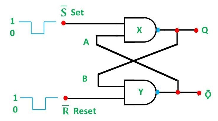
And hey! For you flip flop afficianados we have up here a pair of NAND gates connected into the
classic RS flip flop circuit you always read about in textbooks. So, if you didn't know, you can
build a flip flop from a pair of NAND gates -- now you know. Even more exciting, there is an
arrangement to read the state of this RS flip flop via a read to input port 0x40.
Here is what the classic RS flip flop circuit looks like:
In our case a pair of 3 input NAND gates is being used, they just tie two inputs together to be able to use them as 2 input NAND gates.
It will be interesting to look at the ROM code to see when and why it writes to port 0x40 (note that it will be a write with no particular data, just writing to that port yields the reset). Equally interesting will be to see when and why it might read port 0x40.
Here is my plan. I am going to scan the schematic starting at the upper left, scanning down, then when I get to the bottom, move a bit right and up top, then scan down again.
Tom's Computer Info / tom@mmto.org